'/%3e%3c/svg%3e) Create Project
Create Project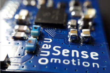
;}.c{fill:%23dbdbdb;}.d{fill:none;stroke:%23333;stroke-linecap:round;stroke-linejoin:round;}%3c/style%3e%3cclipPath%20id='a'%3e%3crect%20class='a'%20width='22'%20height='22'/%3e%3c/clipPath%3e%3c/defs%3e%3cg%20class='b'%3e%3cg%20transform='translate(1.375%202.251)'%3e%3cpath%20class='c'%20d='M7.563,9.224A20.661,20.661,0,0,1,18.8,8.265l-7.088,7.329-.922-.373-.023-3.312-1.389-.741-2.555.389-3.56,2.989-2,1.7s-.1-4.771,6.3-7.021'%20transform='translate(-0.5%200.249)'/%3e%3cpath%20class='d'%20d='M12.174.745l7.332,7.332a.834.834,0,0,1-.017,1.195L12.157,16.2a.833.833,0,0,1-1.405-.606V12.679a.844.844,0,0,0-.931-.832A11.108,11.108,0,0,0,2,16.74a.834.834,0,0,1-1.5-.576C1.132,9.59,3.786,5.4,9.942,5.066a.841.841,0,0,0,.81-.829v-2.9A.833.833,0,0,1,12.174.745Z'%20transform='translate(-0.5%20-0.5)'/%3e%3c/g%3e%3c/g%3e%3c/svg%3e)
Story
Concept & Overview
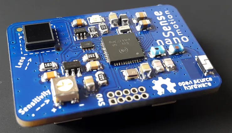
In this project I will present the build of the nanoSense:Motion, an Ultra-Low Power Motion / Human Presence Sensing device with Bluetooth Low Energy connectivity.
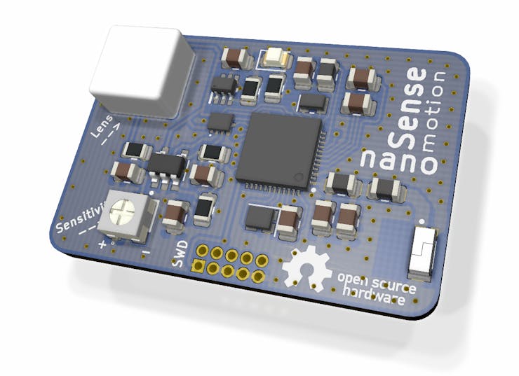
3D render of the device
The device is based on the Kemet PL-N823-01 Pyroelectric Infrared Sensor and the OnSemi RSL10 Bluetooth Low Energy SoC.
The main features of the device are:
Wireless Motion Sensing - battery powered motion sensing with wireless data transmission
Bluetooth Low Energy (BLE) connectivity - motion events are advertised over BLE
Powered from a CR2023 battery - up to 10 years of battery life
Motion Sensing with overall power consumption as low as 1.5 μA @ 3.3V ()
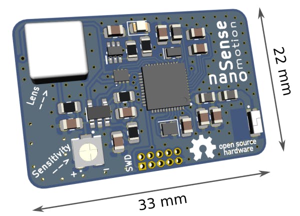
Small form factor - 22 x 33 mm
Power Off mode with 25 nA power consumption
Adjustable Sensitivity - for trade-off between high sensitivity and low current consumption
Support for the Lens used by Kemet SS-430 module
Up to 5m Sensing range (with lens)
(*note: the device is still in PoC stage. Some of the feature are not yet fully functional and some of the proposed specs are not yet met)
The nanoSense:Motion is intended to be used in a Smart Home or a Smart Office. The device can be placed in any room, and it can run from a CR2032 battery for a couple of years.
Using the Kemet PL-N823-01 Pyroelectric Infrared Sensor, along with an ultra-low power amplification circuit, the device is capable is sensing motion with power consummations as low as 1.5 uA @ 3V.
During this time the RSL10 BLE SoC is in sleep mode consuming just about 25nA. When motion is detected the RSL10 is waken up, and an event on Bluetooth Low Energy is advertised.
A Raspberry Pi, or an other Bluetooth Low Energy enabled device used as a Smart Home controller, can listen for these events. Different action like switching on / off the lights can be automatically triggered.
assembled board
Now lets see how this PoC device was built!
Electrical Design
It all started with experimenting with the Kemet SS-430 sensor module. The SS-430 feature the Kemet PL-N823-01 Pyroelectric Infrared Sensor, a sensor capable of sensing motion and human presence by detecting changes in the thermal radiation.
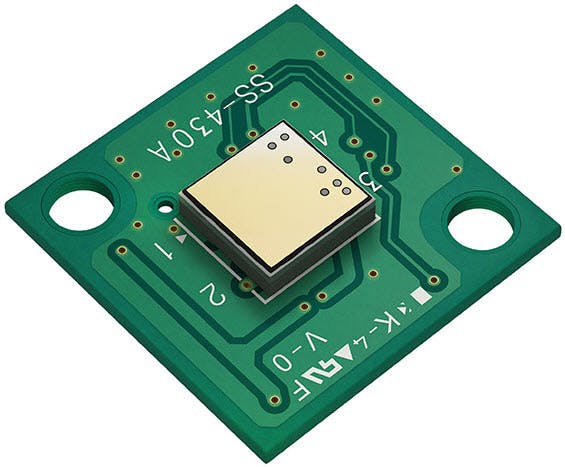
Kemet S3-430 module (without lens)
After fabricating a connector and connecting the module to an Arduino, we can easily detect the pulses generated by the module, when motion is detected.
Although the device is easy to use, its power consumption can be a little bit high battery powered application. For this reason I decided to go with a custom design.
> Signal Amplification
The first step was finding a reference design for the Kemet PL-N823-01 sensor. Unfortunately, there seems to be no such resource on Kemet's website, neither on the PL-N823-01 nor or the SS-430 module's page.
What I found instead is a presentation about Kemet's sensors components. This contains a slide about the PL-N823-01, with an example circuit:
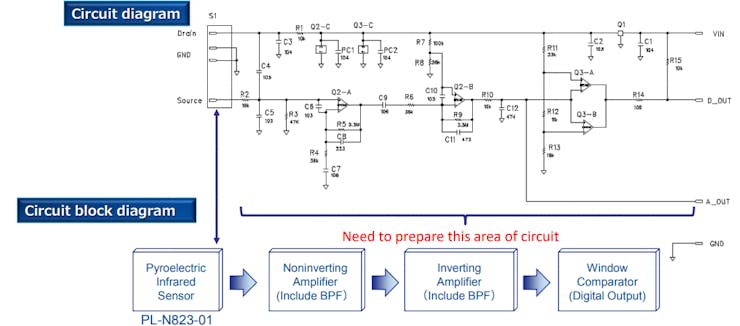
(source: Kemet)
The circuit was a little bit complicated for my competence in analog circuits (too many op-amps :D). Also, the circuit on the SS-430 looked much simpler, so I thought it would worth a try to reverse engineer it.
After some tries I came up with this sketch of the SS-430 signal processing circuit:
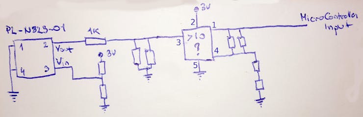
The small rectangular components are resistors and capacitors. The unknown 5 pin IC is probably an op-amp.
Some components / values were still unknown, so I needed to do a little bit of guesswork. Mainly, there was an unknown IC, that we suspected to be an op-amp.
Using an USB oscilloscope, I probed the sensor output and the signal going to the PIC micro-controller:
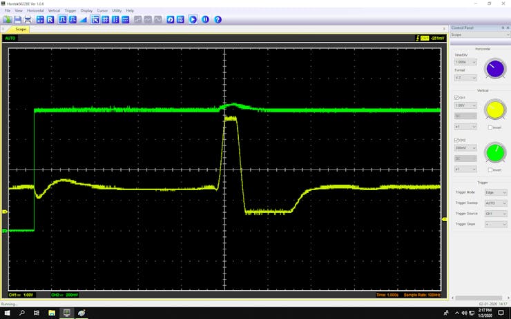
The Green signal is the sensor output, the Yellow one is the amplified signal.
From the oscilloscope output it looks like the sensors produces an output of around 600-800mv, while the circuit from the module is some kind of amplification circuit. When there is no activity the output follows input voltage.
The circuit produces a voltage pulse when the input rises, then the output pulled down to 0V the the input falls back to the original voltage level. After a delay the output will continue to follow the input voltage.
To confirm this I re-created the circuit in LTSpice:
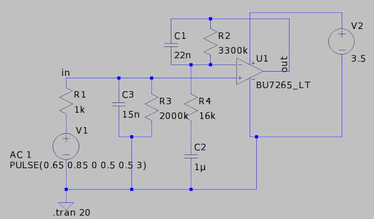
LTSpice circuit, with most of the component values figured out
and the simulation showed a similar output to the one seen on the oscilloscope:
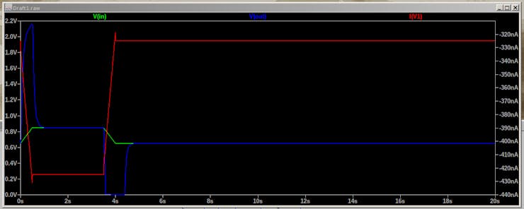
The Green signal is the sensor, the Blue one is the amplifier output. The Red signal show the simulated current consumption of the sensor.
The output signal looked good enough to be processed by a micro-controller, an ADC or an op-amp based window comparator.
> Nano-Power ADC-s
The next step was to find a way to process amplified output.
As I targeted a very low power consumption, using an ADC of a micro-controller was out of the scope. Keeping a micro-controller running all the time would just drawn too much power.
An another option is build a window comparator from two op-amps. I wanted to avoid this, as this would be mean adding two additional op-amps. Also, I'm not too familiar with op-amps, so I probably would have been messed this up.
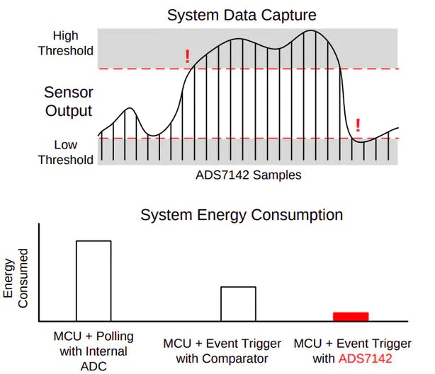
After looking at multiple Analog to Digital Converter (ADC) options, I ended up choosing the Texas Instruments ADS7142.
The ADS7142 is a sensor monitoring IC, with a 12/16-bit ADC and programmable window comparator. Its claims to do autonomous sensor monitoring with a power consumption of just 900 nW.
Its works just like an ordinary ADC, but additionally we can set a low and a high threshold, and the IC will generate an Alert signal whenever the breaches or thresholds. This means we put the micro-controller to sleep mode, with wake-up on the Alert signal, minimizing the power this way the power consumption.
source: Texas Instruments ADS7142 datasheet)
The ADS7142 also have some advanced features like hysteresis and low pass filtering.
> Bluetooth Low Energy / RSL10
As the "brain" of the device I wanted to use a Bluetooth Low Energy (BLE) enabled micro-controller. The SoC devices I considered were the Nordic nRF52x series and the ON Semiconductor RSL10, as I worked with both of these.
Nordic makes multiple devices for Bluetooth and other RF technologies. The most popular ones are the nRF51/52 series. I used these in multiple projects. With the nRF52832 I also did a custom design board, in my Scan Me! - Wire / Contactless Badge board.
On the other hand, my first contact with the OnSemi RSL10 SoC was a RoadTest review I did for it on Element14. What I remarked is the its ultra-low power consumption. The power consumption in sleep mode with wake-up on external signal is as low as 25nA, while even when transmitting over BLE the current consumption stays well bellow 1mA.
As I wanted to achieve a very low power consumption I choose to use the RSL10.
> Chasing Nano-Amps
When I choose the base components of the circuit the main criteria was the power consumption.
The main components consuming power are:
the RSL10 BLE SoC
the Kemet PL-N823-01 sensor
the op-amp used for signal amplification
the Texas Intruments ADS7142 analog-to-digital converter
The RSL10 most of the time is supposed to stay in deep sleep mode with wake up on external signal. The power consumption in this mode is 25nA, which is pretty good.
The power consumption of the Kemet PL-N823-01 is a little bit trickier. The output stage of the sensor is can be seen an N-channel JFET based source follower. The current through JFET is controlled by a DC biasing resistor, connected between the Source pin of the sensor and GND.
The value of this resistor affects both the current consumption and the sensitivity of the sensor. A lower value results in higher biasing current, an thus higher sensitivity. A higher value reduces the current consumption, but may also reduce the sensitivity of the sensor.
To allow a higher degree of flexibility, instead of using a fixed value resistor, I decided to use a 0-2MΩ variable resistor. This way the user can select between high sensitivity and low power consumption.
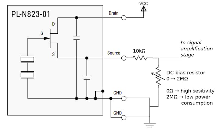
Variable 0-2MOhm resistor setting the sensitivity and current comsumption of the PL-N823-01 sensor
In the terms of op-amp, I selected the op-amp Rohm Semiconductor BU7265SG-TR. This was the general purpose op-amp with the lowest current consumption, available at DigiKey. It has a current consumption of just 350nA.
A feature that wanted to include is the ability to completely power off the analog sub-circuit when the device is not used. Having this means, we can have a power off mode having just the RSL10 staying in deep sleep mode, consuming just a around 25 nA-s.
To implement this a switching device, like a transistor is needed. But, as the current consumption is just a couple of nA-s we need to pay attention to the leakage current of switching device on both the control pin (gate) and power pins.
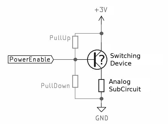
After some research, I decided to go with the Vishay SiP32431 load switch, which claim to have a leakage current of 0.001nA.
Moving the Design to KiCad EDA
After figuring most of the electronics out, the next step was to move the design to Electronics Design Automation Suite.
I like to use KiCad, as it's open source and it's very powerful:
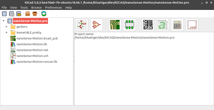
nanoSens-Motion project in KiCad EDA
> Schematics
First start with schematics implemented in Eeschema.
I started with the analog sub-circuit. This is how the final amplification stage looks like:
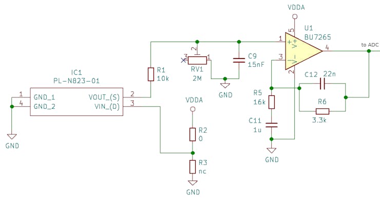
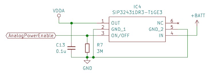
Kemet PL-N823-01 sensor and amplification circuit
The signal from the op-amp goes to the ADS7142 analog to digital converter / sensor monitor. As the ADS7142 has two input available I thought it would be fun to connect raw sensor output to, and see if it can be used without amplification.
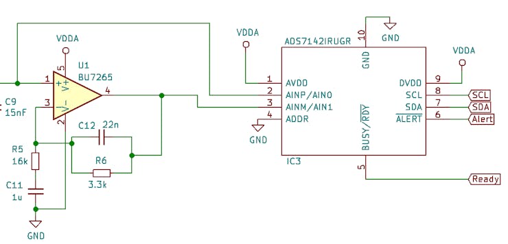
amplified analog signal+ADS7142 ADC
The digital part of the circuit is mainly consisted in the RSL 10 Bluetooth Low Energy SoC and related components.
The design for the RSL10 is mainly based on its datasheet, and the RSL10 reference designs from the ON Semiconductor website.
To reduce the power consumption, the RSL10 is used in a configuration that make use of the internal DC-DC converter of the chip.
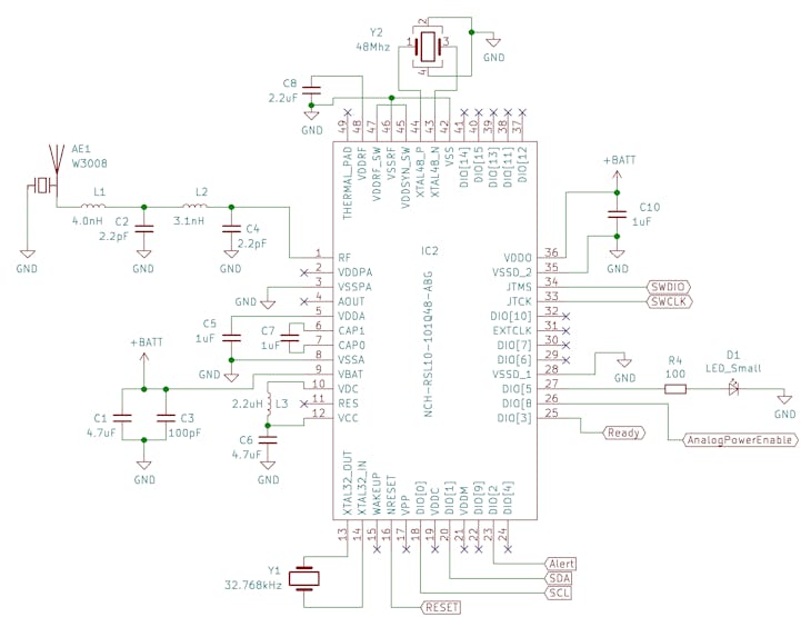
RSL10
The main components of the circuit connected to the RSL10 are:
48 MHz crystal oscillator
32.768 KHz crystal oscillator
chip antenna + impedance matching circuit
status LED
inductor + capacitor used by the DC-DC converter
a couple of capacitor used by the power supply of the IC
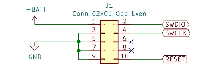
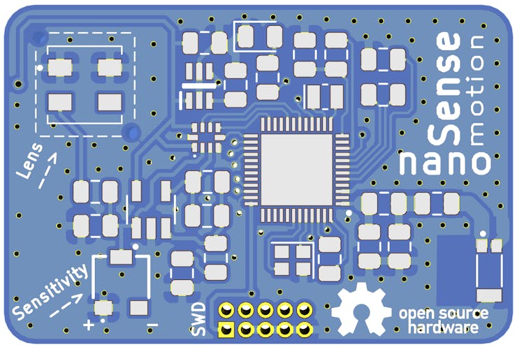
To program the RSL10SoC the JTAG and SWD protocol are available. I decided to go with SWD as it needs a fewer connections:
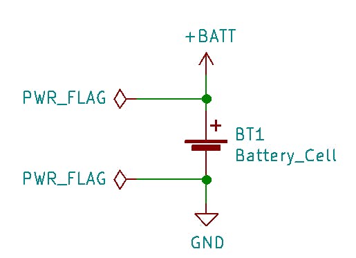
The circuit is powered from a CR2032 battery, with a couple of buffer capacitors added near each component.
The digital part of the circuit is connected directly to the battery, while the analog sub-circuit is powered through the Vishay SiP32431 load switch.
> Selecting Components and Footprints
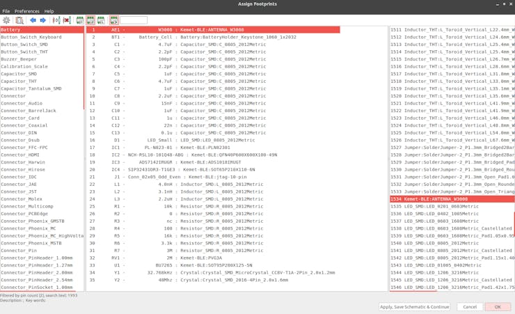
The last step in Eeschema was to assign footprint to components. This is done in the Assign Footprints editor.
Some of the footprint were readily available at the editor. The rest of them I sources from different sites.
These is a summary of footprints used:
the RSL10 comes in a QFN48 package
the PL-N823-01 and the ADS7142 have custom footprint
the SIP32431 and the BU7265 come in fairly standard SOT packages
resistors, capacitors and inductors all have SMD 0805 footprint(I had a lot SMD 0805 resistors and capacitor of them at home. It's also relatively easy to solder)
the battery holder is Keystone 1060 (had one from a previous project)
the chip antenna is a PulseLarsen Antennas W3008 (I choose this because it need a relatively small keep-out area on the PCB)
> PCB Design
The PCB design was done in KiCad Pcbnew:
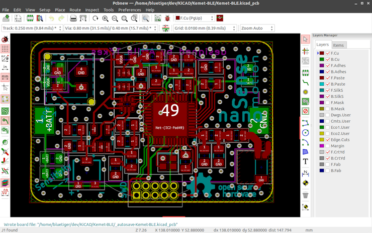
I started with placing the biggest component, the battery holder on the bottom layer, the I draw the outline of the board.
The top layer contains the majority of the components.
I tried to organized the components in multiple sections, keeping each section as well contained as possible.
The section are the following:
Analog sub-circuit
2.4 GHz Radio sub-circuit
Digital sub-circuit
Powering related components
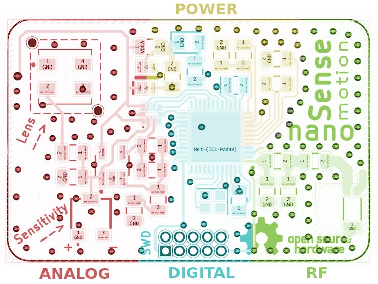
The remaining space, both on the top and bottom layers from a ground plane. The two ground planes are connected with densely places vias.
Here is how the final PCB design looks like:
back side:
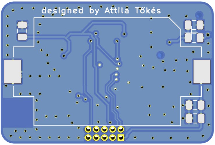
I constantly used the 3D Viewer to ensure nothing is wrong with the resulting PCB. I also used the Design Rule Checker to check the design contains.
After the PCB design was done, I generated the Gerber files and started thinking about the manufacturing.
Soldering & Assembly
After I got the PCB and the parts I started the assembly of the board. I started with the analog sub-circuit, by soldering the Kemet PL-N823-01 sensor, the op-amp, the ADC and the rest of the components.
Then, to do a quick test, I soldered two wires to the analog supply and the ground. After checking that there are no short, I applied 3V and checked that the circuit works.
Next, I continued with the rest of the circuit, the digital part.
This is how the fully assembled board looks like:

After checking for shorts again, I powered the board again. Here the problems stared appearing (Yeah! Hardware is hard :D).
Software & Debugging
The powering up but for some reason was not detected by the SWD debugger (a SEGGER J-Link Lite CortexM). Additionally, at some power-ups the RSL10 started drawing crazy amounts of currents (200-300mA). Looked like it had some trouble with starting up.
At this point at thought the RSL10 was kind of dead. So, I decided to de-solder it, and swap with a RSL10 on development board I have. Surprisingly the IC was still functional.
Next, I soldered the other RSL10 to the nanoSense:Motion and somehow I got it working. I think, I had a bad contact or some bridged pins.
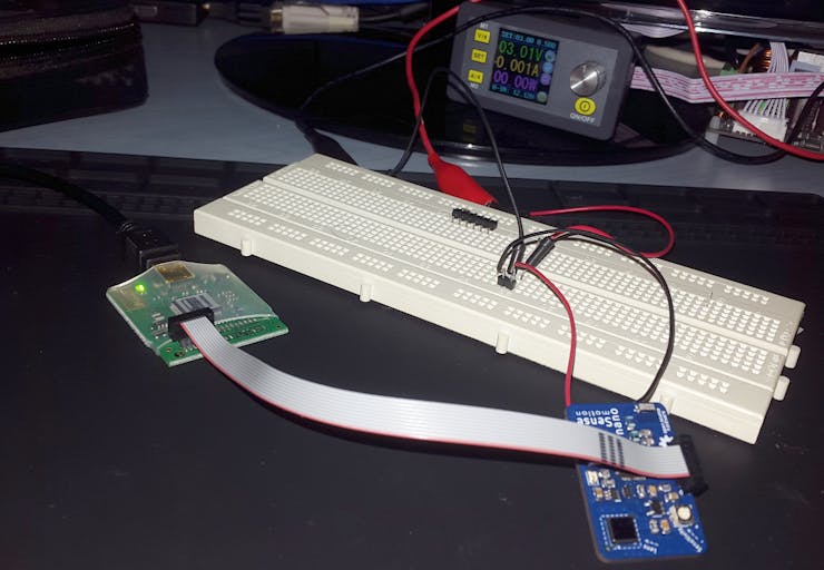
nanoSense: Motion connected to the SWD debugger
As the Software Development IDE the Eclipse C++ can be used.
To set it up:
install Java, J-Link driver
install the RSL10 SDK
install ARM CMSIS package
install ARM FreeRTOS CMSIS package
download & install ON Semi BDK CMSIS package
More details to how to set it up can be found here.
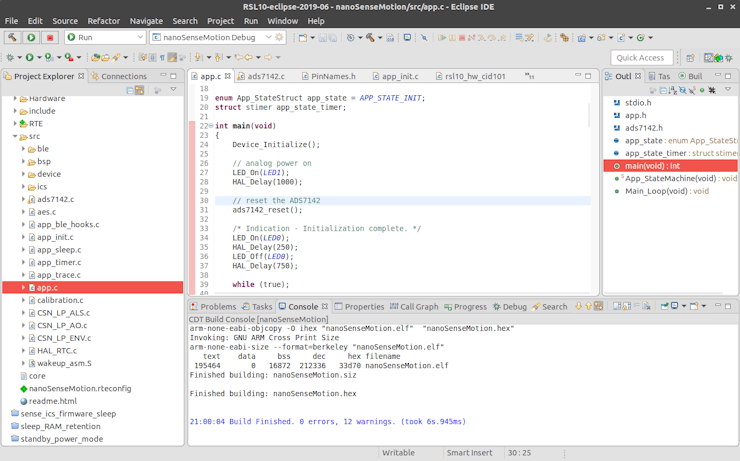
Software in Eclipse C++
The software of nanoSense:Motion is based on one of the ON Semi BDK examples.
After some small modifications, I got a Blinky example running on the nanoSense:Motion. The next step was to try Bluetooth Low Energy communications and Sleep Mode. Both worked fine.
At this point, I faced some issues with the I2C communication ADS7142 and the RSL10. It is probably just a software issue, but needs some investigation. Unfortunately, the I could not reach the I2C signals with an oscilloscope probe, so I could not tell right await wath the problem was.
So, after creating a breakout board for ADS7142, and doing some debugging, it turned out the culprit was just a bad connection between the ADS7142 and the RSL10.
Next, I build a simple library for the ADS7142, and got it working with the RSL 10 app:
ADC values when motion is detected
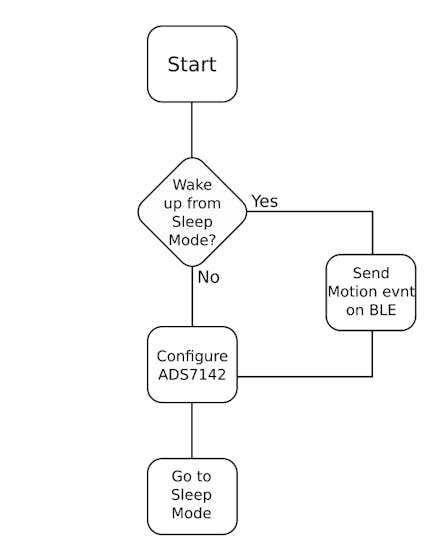
The next step was to use the autonomous monitoring functionality of the ADS7142, so the RSL 10 can stay in sleep mode.
This works as follows:
a reading is done do get an "idle" value for each ADC channel
a high & low threshold is set for each channel
the autonomous monitoring mode is started
the RSL10 is put into sleep mode, with wake up on the alert pin
when the RSL10 wakes up it start advertising over Bluetooth Low Energy (BLE)
the advertising packets can be picked up by a Bluetooth Low Energy (BLE) enabled device, like a Raspberry Pi
Here is how the flow diagram look like like:
The source code can be found in the linked GitHub repository.
Demo
Future Enhancements
First of all I want to fix the software issues and get the nanoSense:Motion fully working.
After this, the plan is take care of the following:
check if the a single stage analog sub-circuit, with just the ADS7142 is feasible(partially done, it looks like working)
optimizing the power consumption of the analog sub-circuit(currently is about 50uA, which is a little bit higher than expected)
impedance matching of the 2.4GHz RF antenna trace, to match the expected 50 Ohm impedance
more software features
References
PL-N823-01 - Pyroelectric Infrared - SMD Proximity Sensor(kemet.com)
SS-430 - Pyroelectric Infrared - SMD Proximity Sensor(kemet.com)
Electronic Components KEMET Charged.® Sensors (kemet.com)
Things to Consider When Designing With the KEMET SS-430 Sensor Module(maker.io / digikey.com)
Unknown 5-pin opamp / comparator IC with “>10” marking(electronics.stackexchange.com)
Switching device for ultra-low power sub-circuit(electronics.stackexchange.com)
Ultra Low-Power Wireless PIR Motion Detector for Cost-Optimized Systems Reference Design(ti.com)
Cheers!
PS: I have a couple of space PCB-s. Let me know if you want some!
;}.c{fill:%23555;}%3c/style%3e%3cclipPath%20id='a'%3e%3crect%20class='a'%20width='18'%20height='18'%20transform='translate(1543%202144)'/%3e%3c/clipPath%3e%3c/defs%3e%3cg%20class='b'%20transform='translate(-1543%20-2144)'%3e%3cpath%20class='c'%20d='M182.144,108.918a.7.7,0,1,1-1.407,0V98.083l-.033.027-.054.05-5.045,5.045a.7.7,0,0,1-1.041-.945l.046-.05,5.045-5.045a2.508,2.508,0,0,1,3.477-.031l.075.072,4.988,5.022a.7.7,0,0,1-.949,1.038l-.05-.046L182.21,98.2l-.066-.061Zm5.394-15.827a.7.7,0,1,1,0,1.407h-12.2a.7.7,0,1,1,0-1.407Z'%20transform='translate(1370.601%202051.909)'/%3e%3c/g%3e%3c/svg%3e "Back to top")