'/%3e%3c/svg%3e) Create Project
Create Project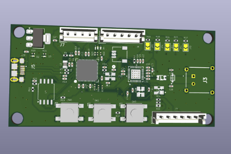
;}.c{fill:%23dbdbdb;}.d{fill:none;stroke:%23333;stroke-linecap:round;stroke-linejoin:round;}%3c/style%3e%3cclipPath%20id='a'%3e%3crect%20class='a'%20width='22'%20height='22'/%3e%3c/clipPath%3e%3c/defs%3e%3cg%20class='b'%3e%3cg%20transform='translate(1.375%202.251)'%3e%3cpath%20class='c'%20d='M7.563,9.224A20.661,20.661,0,0,1,18.8,8.265l-7.088,7.329-.922-.373-.023-3.312-1.389-.741-2.555.389-3.56,2.989-2,1.7s-.1-4.771,6.3-7.021'%20transform='translate(-0.5%200.249)'/%3e%3cpath%20class='d'%20d='M12.174.745l7.332,7.332a.834.834,0,0,1-.017,1.195L12.157,16.2a.833.833,0,0,1-1.405-.606V12.679a.844.844,0,0,0-.931-.832A11.108,11.108,0,0,0,2,16.74a.834.834,0,0,1-1.5-.576C1.132,9.59,3.786,5.4,9.942,5.066a.841.841,0,0,0,.81-.829v-2.9A.833.833,0,0,1,12.174.745Z'%20transform='translate(-0.5%20-0.5)'/%3e%3c/g%3e%3c/g%3e%3c/svg%3e)
This project is using Raspberry Pi RP2050 SoC and Analog Devices ADIN-1111 Single Pair Ethernet chip.
Introduction
In the recent times Internet of Things (IoT) devices are booming. These devices normally operate on radio based wireless technologies such as Wi-Fi, BLE, Cellular LTE-M/NB-IoT or other long-range wireless communication technologies such as LoRa.
Indeed, there is an advantage with wireless technologies that they reduce caballing and installation costs. But the wired technologies are still preferred in tasks that require real-time response. Wired technology is also a good choice for industrial communication and applications where data transfer needs to be happen securely.
Single Pair Ethernet is another wired technology that reduces complexity and works on single pair of twisted pair cables for data transfer. This will reduce the overall data rate than the Ethernet itself but it's useful in applications that do not require very high data rates. The underlying standard for SPE is IEEE802.3cg. The following screenshot from Microchip explains this in detail. It also has distance and data rate mentioned for each substandard.
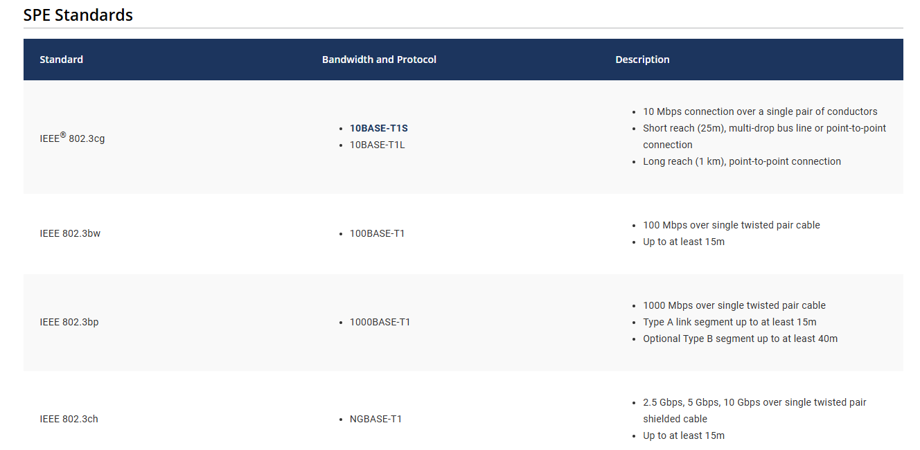
The ADIN-1111 is compatible with 10BASE-T1L standard. Means 10 Mbps data rate and long reach (1 km). Such a long-range point-to-point connection between nodes and data rate is enough for nodes sending sensor data in Industry or smart home applications. These devices need data rate enough to send sensor data that is not that large, but it needs long reach where data can be sent safely and securely in real time.
Wireless technologies such as BLE or Wi-Fi will not have that long range also these technologies are not good for places that have obstacles like buildings. On the other hand, LoRa or even cellular also might have connectivity issues and not ideal choice for real-time secure applications.
Designing with RP-2050
RP-2050 is an ARM Cortex-M33 based processor. It has several peripherals and comes in two different packages (QFN-60 and QFN-80) with pin counts. There is also an option to use RP-2054 which has inbuilt flash chip. This will reduce the component count and need for external flash memory circuit.
For the PCB design most vendors provide some hardware design guidelines and so does Raspberry Pi. For this design I have followed the official Hardware Design Guide.
It is also my suggestion to follow this guide for both the schematic and PCB layout as these designs are complex and needs several iterations that one can avoid with following standards.
You can also follow along my design as this design is working as expected. One question that we normally get even after following the guidelines that is given by the vendor is that ""will it still work""? as we might not have someone who has actually done that and has worked for him/her.
So, this document will explain to you how I have made a working prototype for RP-2050 based PCB design.
Power Supply
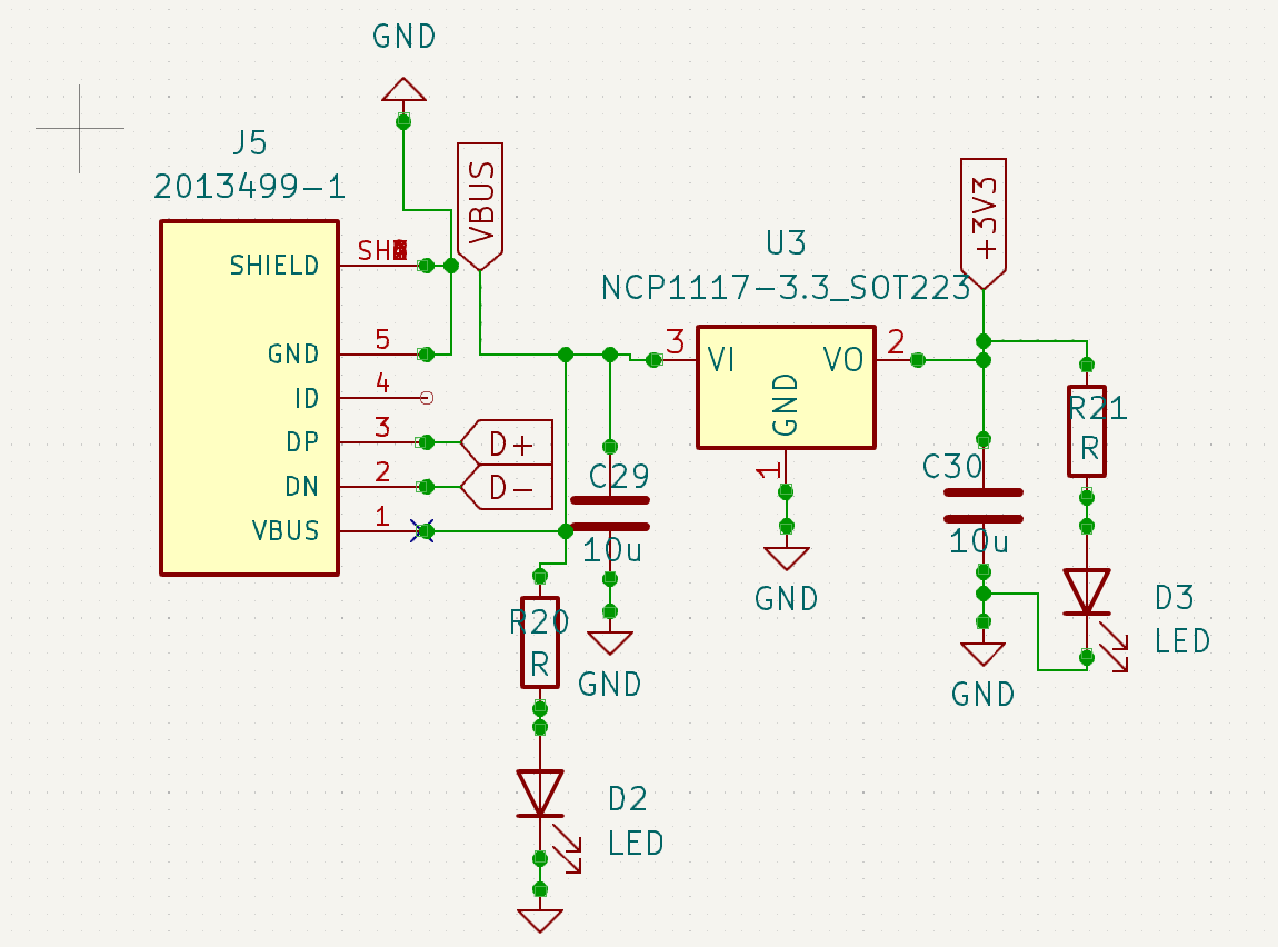
For the power supply to the device, I am using LDO (Low Droupout Regulator). The NCP1117-3.3 is a LDO that can convert 5 V input to 3.3 V output required for RP-2050. I am using micro-USB connector from Texas Instruments. There is also a possibility to use some DC-DC converter to have more power efficient design that can reduce overall power consumption but at the cost of complexity. Hence, I decided to use LDO for the time.
From the schematic diagram you can see the LEDs that I am using on both sides to have visual indication of my power supply chip working as expected. The capacitor on both sides is tantalum capacitor that I have used. These are not the must but the datasheet of the device suggests either ceramic or tantalum capacitors.
It is required to place these capacitors close to the input and output voltage pins of the LDO. This will filter the voltage ripples and give smoot output power to the chip.
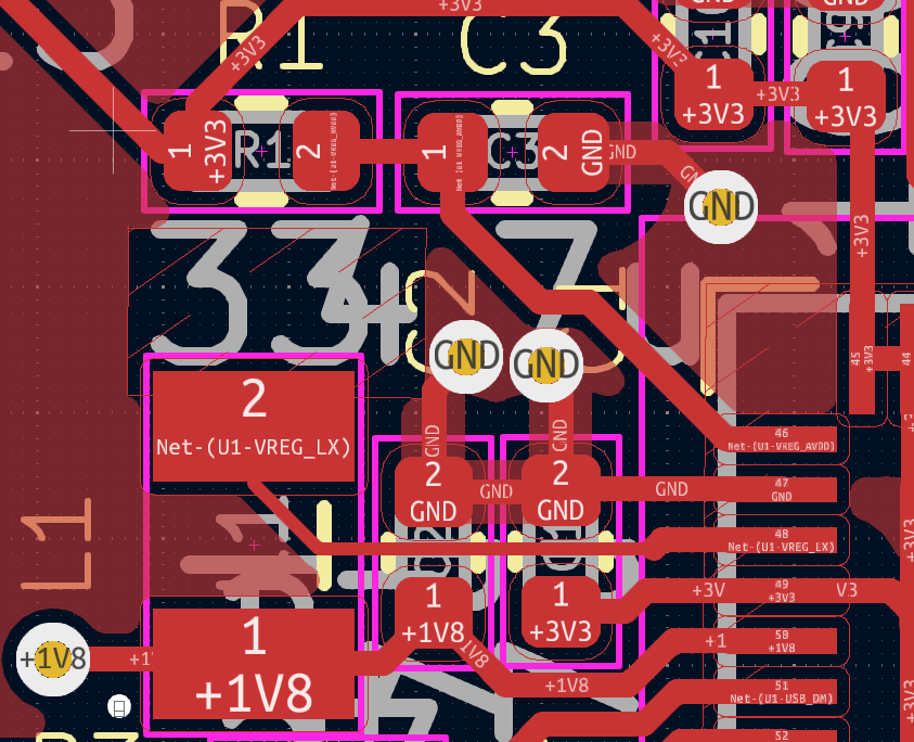
Power domain circuit
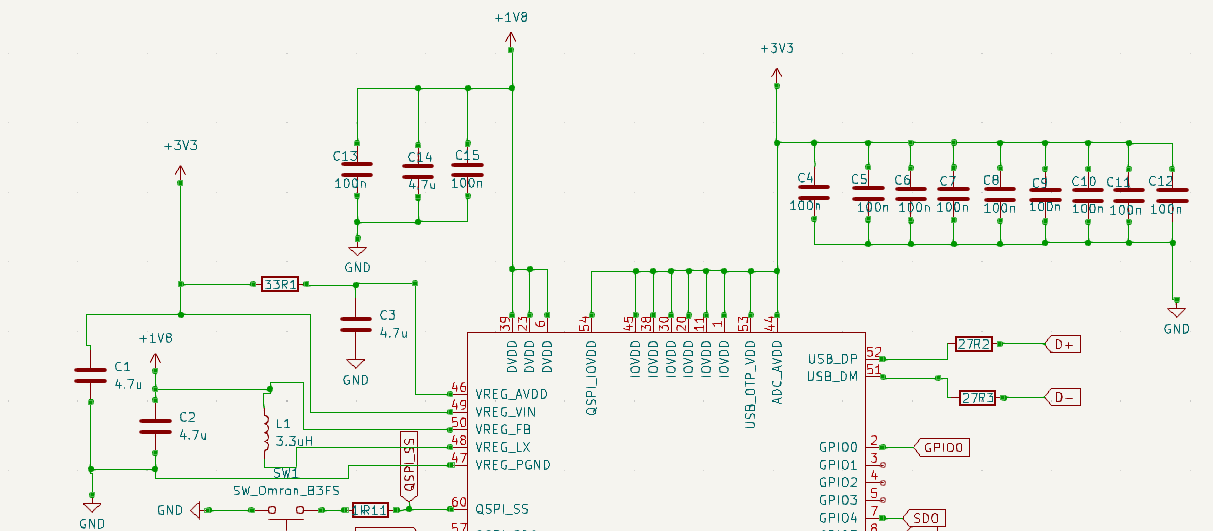
The Hardware Design guidelines suggest using proper layout of the components and its values. Specifically, the placement of components L1, C1, C2 and C3 should be done properly. Above all the L1 inductor has a polarity marking and should be placed as per the marking. The +1V8 marks positive and the other side is negative and should be followed.
Also, the footprint of L1 in KiCaD is different than the default packaging, one should take care of dimensions of the footprint. Ideal is to create one themself.
External Flash Memory
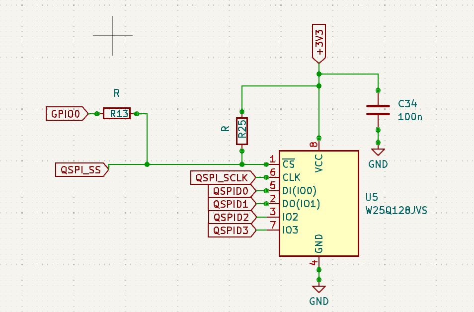
External flash is required to store the application code. Without external flash the device will not be able to run any code. RP-2050 has QSPI interface for external flash devices. As you could see in the image below, the flash is connected over QSPI interface.
I am using Windboard 128 MB QSPI flash chip. But technically you can use any flash chip with even smaller size as per your application requirements. The device is working as expected.
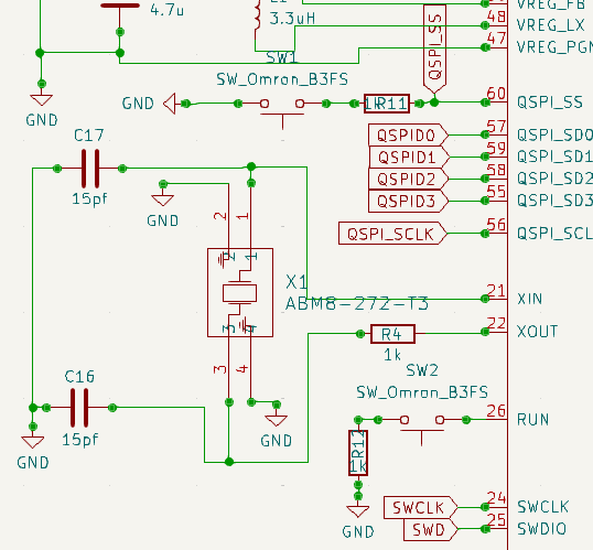
Clock circuit and layout
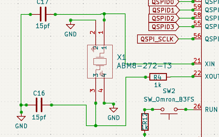
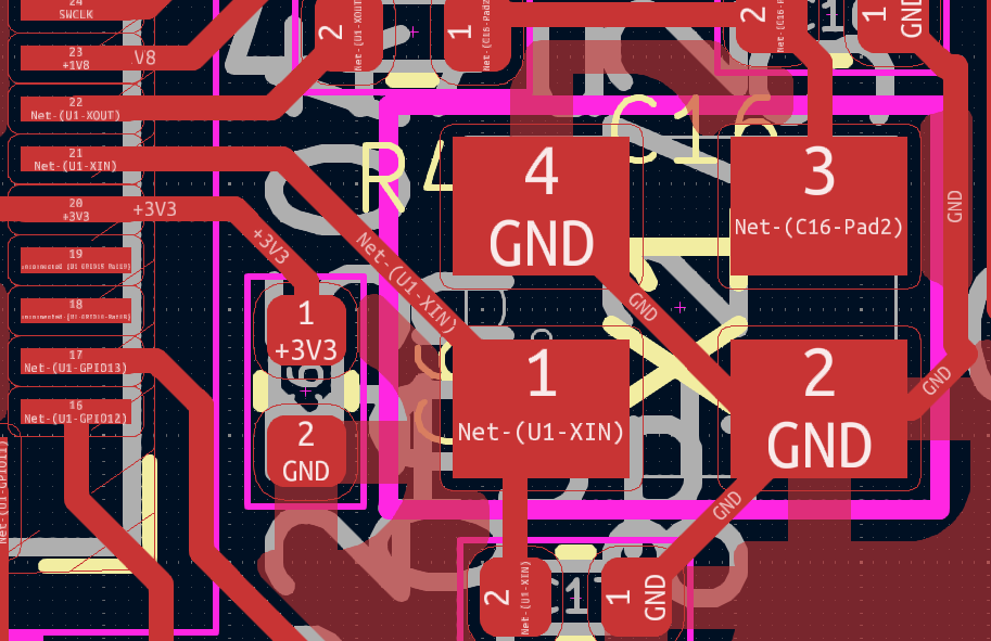
It is possible to power the chip with external clock source on XIN pin. But it is recommended to connect external 12 Mhz crystal on XIN/XOUT pins. Each crystal has Load Capacitance mentioned in the datasheet. That is the capacitance that Crystal needs to operate accurately on its pins.
The official guide suggests using 10 pF capacitors, but I have used 15pf capacitors for the parameters that I have such as parasitic capacitance, Er, etc.
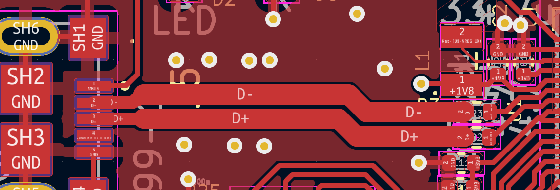
USB interface
Another very important design consideration is USB connection. RP-2050 has on board USB interface that makes it easy to flash new firmware and/or store data. But there is always a layout guideline that must be followed. In this case the differential impedance between the two tracks (D+ and D-) should be 90 ohms.
For this design I have used 0.8 mm wide track with 0.15 mm clearance on 4.2 Er PCB material. The track length is approx. 20 mm. This will give me nearly 90-ohm impedance. One can use KiCaD to calculate this data. It is suggested to not route any unnecessary tracks beneath the USB tracks and minimize via usage in the track. The termination resistance of approx. 27 ohms should be used.
Boot mode selection
Each SoC needs to have Boot mode selection. It is how the SoC knows whether to run the existing code or load a new code on start-up. Boot mode can be selected using buttons.
The SW1 and SW2 in the following schematic is used for the same purpose. The switches can select boot mode or run mode.
Another important thing to notice is to keep SWDIO and SWDCLK pins exposed from the chip to debug the code. It can also help to load the code incase USB interface do not function as expected.
ADIN-1111 schematic and layout
TBD
Man, does it really work? Where is the Proof?
Yes, here it is!
One important question all of us have is whether the final PCB is working or not.
Micro python
Micro python is one of the easiest ways to test a circuit. For this design, I have tested a simple Python code to blink an LED connected on PIN 18,19 & 20 respectively.
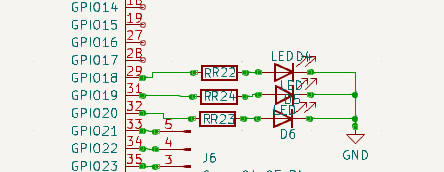
In the following code there are necessary imports for the device. Once that is done I have defined LEDs objects. These objects can then be used in While() loop to turn LED ON/OFF.
from machine import Pin
from time import sleep
# Configure the LED pin (e.g., GPIO2)
led1 = Pin(18, Pin.OUT)
led2 = Pin(19, Pin.OUT)
led3 = Pin(20, Pin.OUT)
while True:
led1.on() # Turn the LED on
sleep(1) # Wait for 1 second
led1.off() # Turn the LED off
sleep(1) # Wait for 1 second
led2.on() # Turn the LED on
sleep(1) # Wait for 1 second
led2.off() # Turn the LED off
sleep(1) # Wait for 1 second
led3.on() # Turn the LED on
sleep(1) # Wait for 1 second
led3.off() # Turn the LED off
sleep(1) # Wait for 1 second
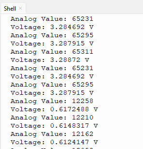
Now, let's try something more. I tried simple ADC functionality of this board.
from machine import ADC, Pin
from time import sleep
adc = ADC(Pin(26))
Then add the code in while() loop to read value and convert this value to mV rating
val = adc.read_u16() # read a raw analog value in the range 0-65535
print("Analog Value:", val)
voltage = (val / 65535) * 3.3
print("Voltage:", voltage, "V")
Grab a wire and connect and disconnect to 3.3V pin and observe the change.
I2C sensor SHT40
I remember that I have had SD-1304 I2C display. But I do not find it at the moment. A good idea would be to make small weather station. Anyways I have connected SHT40 Temperature and Humidity sensor. I found the following code online. It's quite simple and works nice.
i2c = I2C(0, scl=Pin(21), sda=Pin(24))
# SHT40 I2C address
SHT40_ADDR = 0x44
# Function to read temperature and humidity
def read_sht40():
# Send measurement command
i2c.writeto(SHT40_ADDR, b'\xFD')
sleep(0.1) # Wait for measurement
# Read 6 bytes of data
data = i2c.readfrom(SHT40_ADDR, 6)
# Convert the data
temp_raw = int.from_bytes(data[0:2], 'big')
humidity_raw = int.from_bytes(data[3:5], 'big')
# Calculate temperature in Celsius
temperature = -45 + (175 * (temp_raw / 65535.0))
# Calculate relative humidity
humidity = 100 * (humidity_raw / 65535.0)
return temperature, humidity
Temperature: 28.73 °C, Humidity: 69.79 %
Mistakes and learning
There were some mistakes that I have made while making this PCB, but there is still more to learn in the future and such tiny mistakes can help us improve in the future.
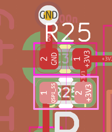
One of the common mistakes I think is about Silkscreen layer and naming of component on that. I wrongly have named Capacitor C34 and Resistor R25. For this reason, the staff might have placed these components in wrong order. (R25 C34 Flipped!). But after receiving the PCB, I realized this and changed these components in right order, and everything started working as expected.
Another mistake that one does not want to see is about power section of the SoC and it's critical. As discussed before there is polarity for L1 inductor and that may have remained unknown to the staff. I had marked this polarity on Silkscreen, but that might have missed. That's why it was in wrong order. But that did not create any issue, but I would suggest anyone do as suggested in hardware design guidelines.
One nice thing that NextPCB does is that they send us the HQ Photos of components soldered on PCB. We can have a careful look on that and suggest an edit.
Conclusion
This PCB design was one of my first's PCBs having SoC on it. Hence, I did not have much detailed experience of it. It is my suggestion to follow the constrains that PCB house mentions in their websites under PCB capabilities section. These constrains should be followed strictly. Otherwise, one might have to redo entire PCB layout work. Which I did several times.
But at the same time, it was a wonderful experience. The flow was to create a PCB schematic and layout design using the Hardware design guidelines. In the meantime, also select the components. Then create a Right BOM material. This is somewhat time taking process, but NextPCB makes it easy using their online component selection tool.
The next part is to Upload the design in that the Gerber, position and drill files to their platform and also if you are doing PCBA then upload the BOM in standard format. This will create an instant Quotation for you. Once it is confirmed by NextPCB you can pay the order total.
The next part is to look for DFM error is there is any. NextPCB has Free Online PCB Gerber Viewer and DFM Tool-NextPCB to do that in advance. Once DFA is done you can keep looking for any engineering questions that you might get.
One day will come and you would realize that your dream PCB is ready.!!
;}.c{fill:%23555;}%3c/style%3e%3cclipPath%20id='a'%3e%3crect%20class='a'%20width='18'%20height='18'%20transform='translate(1543%202144)'/%3e%3c/clipPath%3e%3c/defs%3e%3cg%20class='b'%20transform='translate(-1543%20-2144)'%3e%3cpath%20class='c'%20d='M182.144,108.918a.7.7,0,1,1-1.407,0V98.083l-.033.027-.054.05-5.045,5.045a.7.7,0,0,1-1.041-.945l.046-.05,5.045-5.045a2.508,2.508,0,0,1,3.477-.031l.075.072,4.988,5.022a.7.7,0,0,1-.949,1.038l-.05-.046L182.21,98.2l-.066-.061Zm5.394-15.827a.7.7,0,1,1,0,1.407h-12.2a.7.7,0,1,1,0-1.407Z'%20transform='translate(1370.601%202051.909)'/%3e%3c/g%3e%3c/svg%3e "Back to top")